
Characterization of thin films can be performed to identify properties including the composition, crystal structure, preferred orientation, and film thickness. The MCL has a few thin-film characterization tools, including the X’Pert XRD (x-ray diffraction) and the Hitachi TM 3030+ SEM (EDS or energy dispersive x-ray spectroscopy).
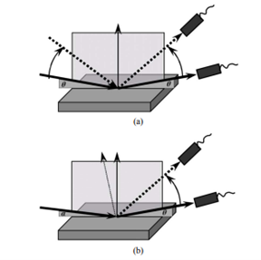
The crystal structure and microstructure orientation of thin film samples can be found with XRD by using the thin film detector on our Philips PANalytical X’Pert, which uses grazing incidence diffraction. Typically, x-ray powder diffraction employs Bragg’s Law, where the incidence angle and the diffracted beam angle are equal as shown in the figure below. In this configuration, both the source and detector move in sync with one another, scanning for constructive interference of the diffracted x-rays.
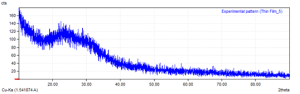
One potential downside is the capability of the x-rays to penetrate into the sample. In order to prevent this, one can use grazing incidence: where the source of the x-rays (or the incident beam) is fixed at a small angle, typically around 1°. This is necessary for thin films to prevent the x-rays from penetrating the film and interacting with the substrate. While the x-ray source is held stationary at the small angle, the thin film detector is free to move around the sample as demonstrated in the figure below.
Using XRD, intensity peaks can be obtained to produce a unique fingerprint to the crystal structures of the sample. In addition ot identification of the material, the microstructure and orientation can be found. Because XRD does not specify the chemical makeup of the sample, prior knowledge of the composition or additional characterization is needed. By using EDS (energy dispersive spectroscopy) on and SEM, the elemental composition of the sample can be determined and used as a search parameter in your search and match software to identify the diffraction pattern. (The MCL has a departmental license to Match! Crystal for peak searching, search and match, and basic Rietveld refinement.)
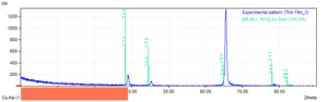
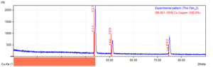
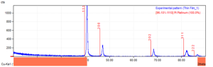
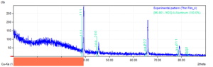
As proof of concept, XRD was conducted on 5 thin film samples that were deposited onto a glass substrate. The elemental composition of these was platinum, copper, gold, aluminum, and carbon. Analysis was performed using Match! software to identify the crystal structure by comparing the diffraction peaks to the Crystallography Open Database, a public database of XRD spectra. The diffraction plots for each of the films can be seen as follows.
For common XRD techniques to be applied, the material in question must be a crystalline material. The deposited carbon was amorphous, and therefore did not produce any diffraction peaks.
The preferred orientation of the microstructure can be determined by looking at peak intensities, which indicate specific crystal planes. For example, the gold film’s (202) plane was more prominent than other peaks in the scan: higher than expected from the database entry. This suggests that a large portion of the crystal structure was grown with that orientation facing outwards. This preferred growth develops during the sputtering deposition process used to make the films.
You can see other examples of other thin films here
Further reading
Written by Jacob High